


专注大空间环境问题解决方案
提供专业通风降温工程方案设计,一站式通风降温工程施工安装服务

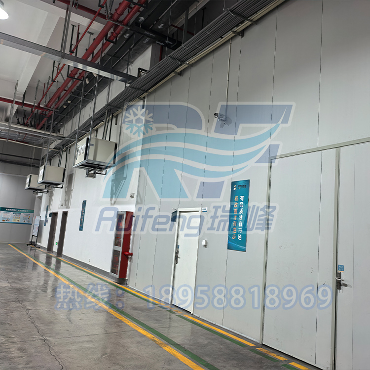
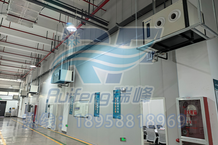
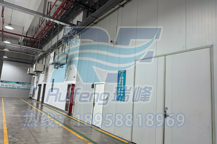
一、项目背景:立足长三角,服务尖端制造
位于浙江嘉兴的跨界半导体公司,是国产半导体产业链中从设计、材料到制造、封测的关键一环。嘉兴地处浙北,属亚热带季风气候,四季分明,夏季高温多湿(平均温度可达28-35℃,湿度常高于70%),冬季阴冷湿润。这种气候对生产环境的恒温恒湿与洁净控制提出了严峻挑战。同时,浙北地区正积极承接长三角半导体产业外溢,聚焦特色工艺与先进封装,形成区域协同的产业布局。该公司依托长三角的区位、人才与供应链优势,正加速推动关键环节的国产化替代。
二、行业洞察:半导体制造与环境控制的共生关系
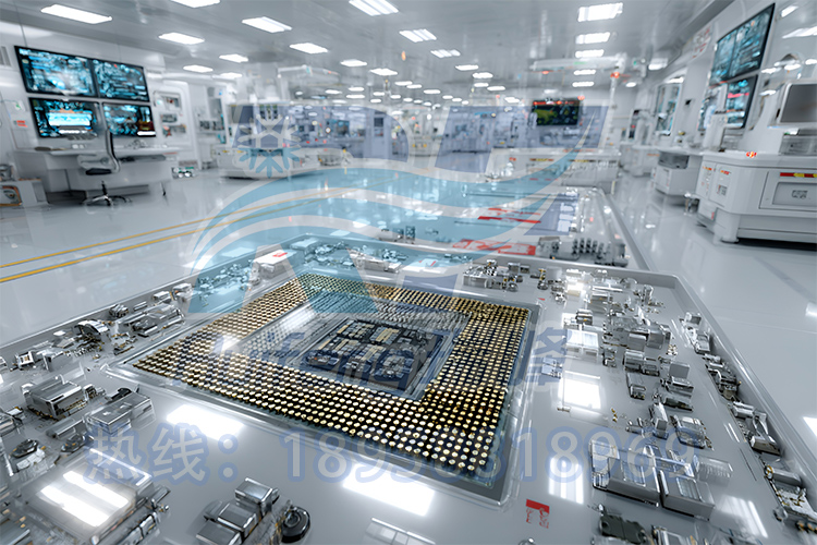
半导体制造是当今世界精度最高、环境最敏感的工业流程之一。其生产环境远非普通“通风降温”所能满足,而是一套融合温湿度、洁净度、气流、微振动及化学污染物控制的尖端工程体系——即“受控环境”或“洁净室环境”。

三、瑞峰从技术本质出发,深入剖析环境与半导体制造的内在关联,形成以下解决方案框架:
(一)、核心关联:环境是半导体生产的“隐形工艺装备”
在纳米级芯片制造中,数百道光刻、刻蚀、沉积工序如同微观世界的“精雕细琢”。环境因素的微小波动,都可能造成整批晶圆的巨额损失。
1、空气洁净度控制——守护纳米尺度的“无尘战场”
技术关联:空气中粒径超过0.1微米的微粒,对于3-5纳米线宽的电路犹如“陨石撞击”,会导致线路短路、断线或图形缺陷。
控制要求:实现ISO 1-5级超高洁净度,确保每立方米空气中超微粒子数控制在个位级别。
方案实现:采用初效、中效、高效/超高效过滤器(HEPA/ULPA)多级组合,结合层流送风设计,形成稳定、均匀的单向气流,迅速排除微粒,确保工作区零污染沉降。
2、温湿度精密调控——工艺一致性的“定海神针”
温度控制:±0.1℃内的波动即可能导致光刻对准偏差,引发层间错位;同时影响刻蚀、沉积等化学反应的速率一致性。
湿度控制:湿度过低(<30%RH)易积聚静电,击穿晶体管栅极;湿度过高则影响光刻胶性能,并加速金属腐蚀。
控制要求:温度常控于22±0.1℃,湿度维持在45±5%RH区间。
方案实现:选用高精度恒温恒湿机组,配合变频调速与智能算法,实时响应工艺热负荷变化,确保环境参数持续稳定。
3、气流组织与压差管理——污染隔离的“气锁防线”
技术关联:通过正压梯度(如5-15Pa)确保气流从高洁净区向低洁净区定向流动,防止交叉污染;对化学机械抛光(CMP)等产污区实施负压控制,遏制污染物扩散。
方案实现:依托精准的风量平衡设计,配合定风量阀(CAV)、变风量阀(VAV)实现动态调控,保障各区域压力稳定、气流有序。
4、微振动与噪声抑制——精密设备的“静音地基”
技术关联:光刻机等设备进行纳米级对准时,微振动会导致成像模糊、定位失准。振源可能来自风机、水泵或外部环境。
方案实现:选用低振动风机与水泵,配备减振基座及柔性接头,优化风管布局以消除气流共振,为设备提供“零干扰”运行环境。
5、气态分子污染物(AMC)控制——隐形缺陷的“分子滤网”
技术关联:空气中微量酸性气体、可凝有机物等会附着晶圆表面,引发电化学腐蚀或薄膜性质变异,导致慢性性能衰退。
方案实现:在粒子过滤基础上,集成化学吸附滤网,针对性去除特定分子污染物,保障工艺气体纯净度与硅片表面完整性。
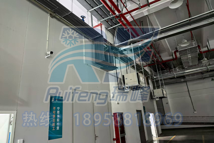
(二)、方案实施:从设备安装服务商到受控环境系统合作伙伴
1、定位升级:从“通风降温服务商”转型为“半导体洁净空间受控环境系统解决方案服务商”,聚焦工艺深度融合。
2、团队构建:组建涵盖半导体工艺、洁净室标准(ISO 14644)及精密控制技术的专业工程师团队。
3、协同合作:与洁净室设计院、总包单位、自控系统服务商紧密配合,专注新风机组(MAU)、风机过滤单元(FFU)、高效送风口及气流组织等核心子系统。
4、数据验证:以实测数据展现系统在温湿度精度、过滤器效率、风速均匀性及振动控制等方面的卓越性能。
5、可靠设计:提供全年不间断运行保障,配置冗余备份与预防性维护体系,确保系统持续稳定。
6、节能优化:集成热回收装置、变频驱动与智能能耗管理,助力客户实现绿色低碳运营。
7、合规认证:所有材料与设备均满足半导体行业防火、低析出、防腐蚀等特殊规范,确保系统自身零污染。
半导体生产环境控制,是多学科技术集成的结晶,直接关乎产品良率、性能与可靠性。本次项目不仅标志着瑞峰成功迈进高门槛、高价值的半导体领域,更体现了我们为客户核心工艺提供深度保障的能力——我们不仅是环境系统的建设者,更是高端制造产业链中不可或缺的价值伙伴。
Ⅰ. Project Background: Based in the Yangtze River Delta, serving cutting-edge manufacturing
A cross-border semiconductor company located in Jiaxing, Zhejiang Province, is a key link in the domestic semiconductor industry chain from design, materials to manufacturing, packaging and testing. Jiaxing is located in northern Zhejiang and has a subtropical monsoon climate with distinct four seasons. The summer is hot and humid (with an average temperature of 28-35 ℃ and humidity often exceeding 70%), while the winter is cold and humid. This climate poses a serious challenge to the constant temperature, humidity, and cleanliness control of production environments. At the same time, the northern Zhejiang region is actively undertaking the spillover of the semiconductor industry from the Yangtze River Delta, focusing on characteristic processes and advanced packaging, and forming a regional coordinated industrial layout. The company is leveraging its location, talent, and supply chain advantages in the Yangtze River Delta to accelerate the localization and substitution of key links.
Ⅱ. Industry Insights: The Symbiotic Relationship between Semiconductor Manufacturing and Environmental Control
Semiconductor manufacturing is one of the most precise and environmentally sensitive industrial processes in the world today. Its production environment is far from being satisfied by ordinary "ventilation and cooling", but rather a cutting-edge engineering system that integrates temperature and humidity, cleanliness, airflow, micro vibration, and chemical pollutant control - that is, a "controlled environment" or "clean room environment".
Ⅲ. Starting from the essence of technology, Ruifeng deeply analyzes the inherent relationship between the environment and semiconductor manufacturing, and forms the following solution framework:
(1) Core correlation: Environment is the 'invisible process equipment' for semiconductor production
In the manufacturing of nanoscale chips, hundreds of photolithography, etching, and deposition processes are like the "fine carving" of the microscopic world. Even small fluctuations in environmental factors can cause significant losses to the entire batch of wafers.
1. Air cleanliness control - guarding the "dust-free battlefield" at the nanoscale
Technical correlation: Particles with a diameter exceeding 0.1 microns in the air are like "meteorite impacts" on circuits with a line width of 3-5 nanometers, which can cause short circuits, wire breaks, or graphic defects in the circuit.
Control requirement: Achieve ISO 1-5 ultra-high cleanliness, ensuring that the number of ultrafine particles per cubic meter of air is controlled at the level of units.
Solution implementation: Adopting a multi-stage combination of primary efficiency, medium efficiency, and high-efficiency/ultra high efficiency filters (HEPA/ULPA), combined with laminar air supply design, to form a stable and uniform unidirectional airflow, quickly eliminate particles, and ensure zero pollution settlement in the working area.
2. Precise control of temperature and humidity - the "sea fixing needle" for process consistency
Temperature control: Fluctuations within ± 0.1 ℃ may cause alignment deviation in photolithography, leading to interlayer misalignment; Simultaneously affecting the rate consistency of chemical reactions such as etching and deposition.
Humidity control: If the humidity is too low (<30% RH), static electricity can accumulate and break down the transistor gate; Excessive humidity can affect the performance of photoresist and accelerate metal corrosion.
Control requirements: The temperature should be kept at 22 ± 0.1 ℃, and the humidity should be maintained within the range of 45 ± 5% RH.
Solution implementation: High precision constant temperature and humidity units are selected, combined with variable frequency speed regulation and intelligent algorithms, to respond in real-time to changes in process heat load and ensure continuous stability of environmental parameters.
3. Airflow organization and pressure difference management - the "air lock defense line" for pollution isolation
Technical correlation: By using a positive pressure gradient (such as 5-15Pa), the airflow is directed from the high clean area to the low clean area to prevent cross contamination; Implement negative pressure control on contaminated areas such as chemical mechanical polishing (CMP) to curb the spread of pollutants.
Solution implementation: Based on precise air volume balance design, combined with constant air volume valve (CAV) and variable air volume valve (VAV) to achieve dynamic control, ensuring stable pressure and orderly airflow in various areas.
4. Micro vibration and noise suppression - the "silent foundation" of precision equipment
Technical correlation: When using equipment such as lithography machines for nanoscale alignment, micro vibrations can cause imaging blurring and positioning errors. The vibration source may come from fans, water pumps, or external environments.
Solution implementation: Select low vibration fans and pumps, equipped with vibration reduction bases and flexible joints, optimize duct layout to eliminate airflow resonance, and provide a "zero interference" operating environment for the equipment.
5. Control of gaseous molecular pollutants (AMC) - a "molecular filter" for invisible defects
Technical correlation: Trace amounts of acidic gases and condensable organic matter in the air can adhere to the surface of wafers, causing electrochemical corrosion or changes in film properties, leading to chronic performance degradation.
Solution implementation: On the basis of particle filtration, an integrated chemical adsorption filter is used to remove specific molecular pollutants in a targeted manner, ensuring the purity of process gases and the integrity of silicon wafer surfaces.
(2) Implementation of the plan: from equipment installation service providers to controlled environment system partners
1. Positioning upgrade: Transforming from a "ventilation and cooling service provider" to a "semiconductor clean space controlled environment system solution service provider", focusing on deep integration of processes.
2. Team building: Establish a professional engineering team covering semiconductor processes, cleanroom standards (ISO 14644), and precision control technology.
3. Collaborative cooperation: Work closely with cleanroom design institutes, general contractors, and automation system service providers to focus on core subsystems such as fresh air units (MAUs), fan filtration units (FFUs), efficient air supply outlets, and airflow organization.
4. Data validation: Demonstrate the outstanding performance of the system in terms of temperature and humidity accuracy, filter efficiency, wind speed uniformity, and vibration control through measured data.
5. Reliable design: Provide year-round uninterrupted operation guarantee, configure redundant backup and preventive maintenance system to ensure continuous stability of the system.
6. Energy saving optimization: Integrating heat recovery devices, variable frequency drives, and intelligent energy management to help customers achieve green and low-carbon operations.
7. Compliance certification: All materials and equipment meet special specifications for fire prevention, low precipitation, and corrosion prevention in the semiconductor industry, ensuring zero pollution of the system itself.
IV. Conclusion
Semiconductor production environment control is the culmination of multidisciplinary technology integration, directly impacting product yield, performance, and reliability. This project not only marks Ruifeng's successful entry into the high-threshold, high-value semiconductor field, but also demonstrates our ability to provide in-depth support for our customers' core processes - we are not only builders of environmental systems, but also indispensable value partners in the high-end manufacturing industry chain.
更多案例


客服热线:18958818969
服务热线:13356130717
电子邮件:ruifeng0717@163.com
公司地址:浙江省温州市平阳县万全镇紫来创业园二幢
瑞峰官网:www.wzrfhb.com


长按屏幕识别二维码
打开手机扫描二维码


